INTENGENT delivers fabless InP PIC services by utilizing its flagship taper-assisted vertical integration (TAVI) Platform. Based on a regrowth-free process, it allows for design to manufacture with volume scalability.
Platform
III-V semiconductors epitaxially grown on InP substrate, uniquely, allow for all the active and passive functions expected from PICs, while covering the major communication O-, S-, C-, and L-band wavelength ranges. That naturally makes them the materials of choice for a monolithic photonic integration in tele- / datacom applications and beyond.
In the monolithic photonic integration, different devices, processed from different materials, should be combined onto one substrate and optically interconnected. This is a challenging problem and has no simple generic solution, for which reason InP PICs remain largely a non-standardized, highly divergent, and hard to access boutique technology.
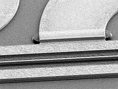
Taper-assisted vertical integration (TAVI) is a regrowth-free photonic integration technology that raises to the challenge, by providing a platform for InP PICs, in which the standardized manufacturing process is applied to generic design solutions implemented in the industrial grade foundry.
The device library includes distributed feedback lasers, electro-absorption and Mach-Zehnder modulators, semiconductor optical amplifiers, and photodetectors - on the active side, and beam splitters / combiners, wavelength division (de)multiplexers, multi-mode interferometers, spot-size converters, and various elements of the waveguide circuitry - on the passive side. It covers applications from high-speed data center interconnects to microwave photonics, based on the same process design kit (PDK).
The key to the TAVI Platform is decoupling of the epitaxial growth and wafer fabrication, enabling for outsourcing each of them to a respective commercial foundry. The TAVI Platform's materials and fabrication processes are, by and large, the same as those used in III-V analog electronics. This allows for fabless PICs via the same food chain as MMICs - a much higher volume production for a much larger market.
Delivery
To facilitate the fabless InP PICs based on the TAVI Platform, a Consortium of INTENGENT (the technology provider), Global Communication Semiconductors (GCS, the wafer fabrication foundry), and VLC Photonics (VLC, the PIC design house) has been established, in which:
INTENGENT brings a wealth of expertise in the vertical integration, including PIC's epitaxial structure, functional waveguide, and building block design, along with decades of experience in InP PIC development and productizing for the tele- / datacom markets;

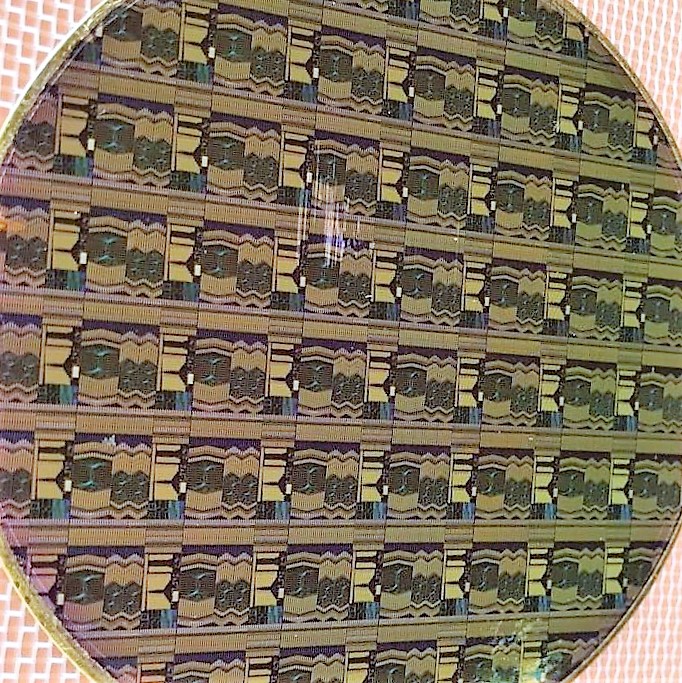
GCS, a leading III-V wafer fabrication foundry serving the markets from wireless to opticom and running tens of thousands 4" / 6" wafer starts per year, provides an industrial grade process in ISO 9001 certified facility, adjusted to the TAVI PIC fabrication on 4" InP wafers;

VLC, a reputed PIC design house with a track of records of PDK development and circuit design in different material / technology platforms, puts in a great deal of expertise in building, verifying, and using PDK.
Collectively, we deliver a one-stop, turn-key fabless InP PIC solutions, by providing:

- The application assessment;
- The PIC definition and design;
- The supply chain management;
- The chip fabrication and testing.
From the proof of concept to prototyping to volume-scalable manufacturing - all in the same platform, thru the same food chain, by using the same process, equipment, and PDK.